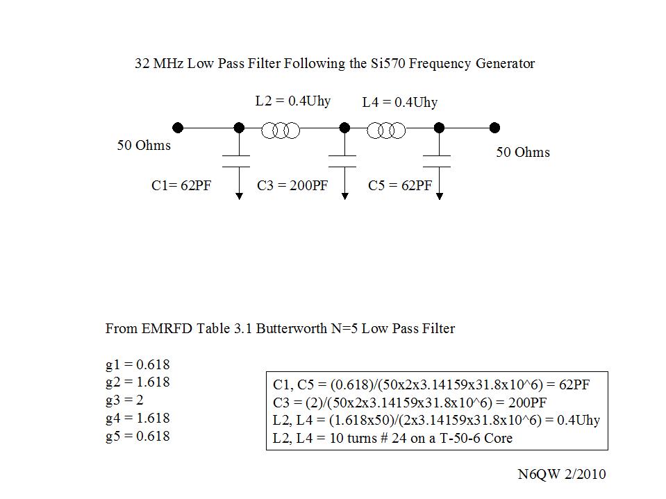
Project Description The idea for a small, shirt pocket sized QRP SSB Transceiver goes back prior to 2007 when I made an attempt at such a project using through hole devices and homebrew crystal filters. Much valuable insight and experience was gained from that effort. From those experiments I successfully built two transceivers, one for 17M and one for 40M. These can be seen HERE, These were single conversion transceivers employing a 4.9152 MHz IF. A novel solution was found for frequency control in the case of the 17M model, in that standard computer crystals were utilized in a wide range VXO placed above the IF. Super stability and a 40 KHz frequency excursion made for some very pleasant QSO's. Several critical conclusions were reached in those projects chief among those that bi-lateral amplifiers worked very nicely in such a transceiver architecture and secondly -- it would be fairly difficult to build a shirt pocket sized transceiver with through hole components especially where "manhattan" style construction was employed. That said I did not give up hope for shrinking down the size of the transceiver. Early in 2009, I built a tri-band dual conversion QRP SSB Transceiver. This was a fun project in that it employed the frequency scheme and architecture of the Heathkit HW/SB series transceivers right down to the crystal filter, carrier oscillator crystals and heterodyne crystals. For good measure the radio even has a Heathkit "S" Meter. Just to be fair the radio does have a Ten Tec PTO. A good deal of DX was worked with this radio and from that many new things were learned by this old dog. The band switching for the bands (40, 20 and 15M) is all done with DC using either diode steering or small board mounted relays. That radio can be seen HERE. This is definitely not a shirt pocket sized transceiver as it measures 1/2 a cubic foot. In the fall of 2009 a planned vacation trip prompted the idea of a small shirt pocket sized receiver so I could sort of keep in touch with what was happening. My first choice was a small regenerative receiver which I built and got working only to bring back memories of why I quickly moved to superhets with good filters and not so touchy tuning. I then remembered that I had purchased some communication MMIC devices from Watkins Johnson (now TriQuint) and had them stored away somewhere. I retrieved them and in about a half hour had a design. The whole receiver was on a board 3" X 4". Now we are shirt pocket sized. Three MMIC devices (TriQuint AG303-86G) were used in that design including an untuned RF amplifier, a post mixer amplifier following an SBL-1, an IF amplifier following a homebrew 4 pole crystal filter at 5.185 MHz. The Product Detector/Carrier Oscillator is a SA602, followed by an LM386-3 for the audio stage. For the LO, I initially tried a SA602 as a VXO using standard 12.28 MHz Crystals but found I could not get into the 40M CW band. I then hit on the idea of converting the SA602 to a 1.8 MHz VTO. That worked nicely! But the level was too low for the SBL-1 so a 2N2222A configured as a strong amplifier was used to boost the signal level. Well there I had it! A really small, high performance receiver, all on one board and it was shirt pocket size! Well it didn't take more than 30 seconds of thought to steer me into building a companion transmitter which could be built on the same sized board and use the VTO as a common circuit element. A NE555 and a PNP power transistor did the heavy work as a TR switch. In short order, I had a working CW transceiver. Yes the transmitter also uses one TriQuint AG303-86G MMIC Device. I stacked the boards one on top of each other and that made for a small footprint. The complete transceiver measures 3X4X2.5 Inches. A little fat for shirt pocket size but getting closer. This radio is good for 6 watts output and has had a good account for itself. It can be seen HERE. This project proved that MMIC's could be utilized in future designs and it also gave me some experience using Surface Mount Devices --something I have been avoiding for a long time. At 68, the eyes are not too good and the hands not too steady. One major tool has proved to be invaluable in the various recent projects and that is a mini-milling machine. With this bench mounted tool I am able to mill away copper material that conforms to the circuit parts and signal flow. This project was the first time I was able to mill a circuit to accept the SOIC8 standard. Using a 1/32 end mill and laying out the board in 5 MM squares this readily facilitates surface mount components down to the 0805 standard. Typically the total elapsed time from laying out the circuit to having a milled board is now down to about a two hour turnaround -- and no messy chemicals! Enter the MMIC Based 20 Meter QRP SSB Transceiver There is one thing about hams -- we can't leave well enough alone! Based on the successful 40M MMIC CW Transceiver Project, my thoughts turned back to my quest for a shirt pocket sized QRP SSB Transceiver. Thus this project has a focus to shrink the size of a QRP SSB transceiver based on some of my recent successful projects. Design Criteria: * Single Conversion with 9.0 MHz Commercial Crystal Filter and 5.0 MHz VTO * Bi-Lateral Stages (3 of them) using the AG303-86G MMIC's which are diode steered * Use of the lower power Double Balanced Mixer for the Product Detector and the Balanced Modulator as well as the Tx & Rx Mixer, Mini-Circuits Labs ADE-1L (3dBM Device) * At least 1 watt output. * RF Gain Stage * Small Size * Stable VTO (May require a fast frequency stabilizer) My initial thoughts about the MMIC Gain Block Amplifier was a singular device which could be used both in the transmit and receive mode such as was done on many of my earlier projects utilizing dual gate MOSFET or J310's arranged in cascode fashion. I convinced myself that for the small additional cost that utilizing separate devices with diode steering may actually cause fewer problems. Don't forget the AG303-86G's are good from 0 to 6000 MHz and have a gain of 20+ DB. I had initially contacted TriQuint about the use of MMIC's in the 40M CW transceiver and received an email reply from John WB1ALZ. In a subsequent email to WB1ALZ, I inquired about the use of the MMIC's in a diode steered bi-directional amplifier. With my inquiry I provided a proposed circuit diagram. John responded that the MMIC's could be used in this fashion and made several circuit change suggestions. These have been incorporated in the final design. The current design uses three such pairs of amplifiers. One set is used after the 14.0 MHz Band Pass Filter. A second set follows the Rx/Tx Mixer (ADE-1L) and feeds the 9.0 MHz 6 Pole Crystal Filter. The third set follows the Crystal Filter and feeds another ADE-1L which is used as the Product Detector on Receive and Balanced Modulator on Transmit. The input/output impedance of the MMIC pair is 50 Ohms which is a perfect match for the Band Pass Filter and the ADE-1L's. The Crystal Filter (available from the GQRP Club or contact Bill Kelsey N8ET) has a 2.2 KHz wide bandwidth and the input/output impedance is 500 ohms. To match the filter to the MMIC bilateral amplifiers I wound matching transformers on FT 37-43 Ferrite Cores. A 50 to 500 Ohm match entails a 10:1 transformer. This is easily done with a 4 turn to 13 turn winding. (4^2 = 16, and 13^2 = 169, 169/16 ~ =10). The GQRP filter has since been swapped out with a Yaesu 8 Pole filter thus providing slightly better shape factor. The In/Out impedance is still 500 Ohms and the installation footprint is the same, so this change is essentially a drop in component switch. The Audio Amplifier stage is somewhat different from what I have previously used. Typically previous audio stages used an NE5534 Pre-Amp driving an LM386-3. With board space being limited, I experimented with a single 2N3904 as a pre-amp stage and followed that with the LM386-3. That proved to be a good combination as the output level is ear splitting. With the RF pre-amp "On" --strong stations easily drive an 8 Ohm six inch speaker to something beyond very loud. For the Microphone amplifier I used the NE5534. I am still experimenting with the value of the coupling capacitor and find that the Hi's tend to prevail. I need to get some Lo's in there. More opportunities. The VTO has once again proved to be an interesting trade-off with a small size and no tuning capacitor. Initially I used a cheapo Radio Shack 10K Linear pot. With the circuit constants I selected the VTO tunes 200 KHz. Well you can imagine how touchy the pot is --you have to be very adept to tune in a station. I have since purchased and upgraded that pot to a Bourns 10K ten turn linear wire wound pot. Much better. The VTO did tend to drift and I now have PIC Microcontroller (16F88) Fast Stabilizer in line and while that looked very promising that has proved otherwise. I just have not been able to determine the proper values of biasing resistors so that drift is corrected without large correction swings. The first LO was my DDS-60 but the spurs are an issue and it seems to have a problem on transmit with RF feedback! By and large the best solution has been to use the Drake TR7 PTO which unfortunately does not aid the quest for a shirt pocket sized transceiver. This PTO was purchased for another project. The TR-7 PTO is very stable and for home use is ideal ~ large tuning knob and very stable! --------------------------------------------------------------------------------------------------------------- VTO Update as of 1/28/2010 In mid January 2010 I was made aware of a Si570 frequency generator kit available from K5BCQ see the following URL ( http://www.qsl.net/k5bcq/Kits/Kits.html). This kit costing around $40 plus shipping is simply amazing! I have installed the kit and am very pleased with the result and the unit can be seen HERE. The actual frequency generator board is slightly smaller than my VTO board and the bonus is a very large display. The output from the generator is 3 volt Peak to Peak square wave (See the waveform HERE) which was conditioned using a 10 dB Pi Type Pad consisting of two 100 ohm resistors for the parallel elements and 62 ohms for the series element. The Low Pass Filter following the Pad is used to clean up the square wave and turn it into a sine wave. This is easily done with two 680 PF caps for the outer two caps and the common cap is a 1000 PF. Two inductors comprised of 21 Turns of #24 enamel wire wound on a T-44-6 Iron Powder Ferrite Core complete the network. The conditioned waveform can be seen HERE. Several modifications have been made to the Si570 Frequency Generator Kit. The first has been to program all of the offsets so the LO signal is ABOVE the operating frequency by 9.0 MHz. Thus for an operating frequency of 14.2 MHz the LO outputs at 23.2 MHz (the display reads 14.2 MHz). The reason for this is to provide the capability to essentially operate on all of the ham bands yet have the frequency display read the correct band. As an example for 160M the LO is operating at 11.0 MHz and for 15M operation the LO is operating at 30 MHz. By placing the LO above the operating frequency has significant advantages with regard to harmonics and unwanted mixer products. This has been well documented in publications such as EMRFD. I opted to not include 10M operation and thus my Low Pass Filter has been designed for a cut off frequency of 32 MHz. This can be seen HERE. The other modification was to bypass the board mounted Mechanical Encoder that comes standard with the kit. This board mounted encoder is not convenient for mounting on a front panel and very likely was not intended for constant use such as you would have in "spinning the dial". The Mechanical Encoder also has a built in "push in" type switch that is used for various applications such as set up and moving through various memories. That too most likely was not deisgned for constant use. After some investigation I came up with a circuit to substitute a more rugged optical encoder and a separate momentary push button switch arrangement. This has proven to work exceptionally well for this application and is currently installed in the radio. The modification can be seen HERE. --------------------------------------------------------------------------------------------------------------- I have also built a 5.185 MHz VXO and while that is very stable the relatively low frequency of the crystals makes frequency excursion on the order of only a few KHz. One combination currently in the breadboard stage but not been tried and that is to use Crystals in the 13.5 MHz range in a Super VXO configuration combined with a small separate crytsal oscillator running at 8.3 MHz resulting in a difference frequency of 5.2 MHz. The same SA612 could be used as a combo VXO and frequency mixer with a 2N3819 used as the external 8.3 Mhz Oscillator. Two 13.5 MHz crystal have yielded a 10 KHz excursion and with several more crystals in parallel quite possibly a 40 KHz excursion could result. That would be sufficient for a pocket sized device. I have already made some modifications to the receiver input. On strong stations the high gain 2N2222A RF Amp overwhelmed the radio. I then added a pot in the emitter lead which could act as an RF gain control. That helped but the final solution was to include a really small SPDT slide switch where the center contact is connected to the board mounted relay that is used as a part of the TR sequence. In one position the low pass filter is connected to the 14 MHz Band Pass Filter (through diode steering). In the other position the low pass filter is connected to the 2N2222A RF Amp. That is far better than try to adjust a pot. It works really well -- and it is dramatic how much gain a single 2N2222A can provide! I have purchased some really tiny SPDT 5VDC relays and in a final configuration the SPDT slide switch would be replaced with the relay thus enabling a front panel control of having the Receiver RF Amp "on" or "off". I also have modified the Carrier Oscillator circuit. Previously the Carrier Oscillator was comprised of a 2N3819 FET oscillator followed by a 2N3819 Amplifier and then a AG303-86G MMIC amp stage took on the chore to deliver several volts of RF to the ADE-1L. There simply was too much signal to the ADE-1L. I removed the second 2N3819 and now the oscillator feeds the MMIC stage and there is plenty of drive the DBM. Less parts is always good! A nagging problem involves where the carrier oscillator is placed on the Crystal Filter pass band. For a 9.0 MHz Center Frequency, the usual USB oscillator is set for 8.9985 MHz. That has been done with several crystal filters and several oscillator crystals. Placement at this frequency makes incoming signals sound very nice but on transmit there is an obvious presence of a carrier. Shifting the carrier frequency until no carrier output is observed or heard results in the "pinched nose" signal on both transmit and receive. At first I thought this was the too much drive problem with the second 2N3819 in line. If the problem still persists, I have developed a configuration of an SBL-1 where an external balance pot can be included in the circuit.Thus I may have to shift to the SBL-1 if I am unable to resolve the carrier issue with the ADE-1L. Upon further investigation the carrier oscillator was switched out and that since has cured this issue. [The SBL-1 is an 8 pin device where access can be gained to the internal transformers. My experiments have indicated a small 100 to 200 ohm pot can be connected across pins 5 and 6 of the SBL-1 and the center wiper on the pot is connected to ground. The carrier balance can be finely tuned in this manner. That said this also provides a means for unbalancing the carrier such as would be required for tune up purposes. A 22 ohm resistor is connected to either Pin 5 or 6 and to enable tune up is simply grounded. In the case where the SBL-1 maybe located near the front panel a DPST switch is used to ground the resistor while at the same time the second set of contacts is used to key the PTT. If the SBL-1 is further away then a small board mounted DPST relay is used for that purpose. That is how the Tri-Band transceiver is placed into "tune". Once the 22 ohm resistor is connected to the circuit, but left ungrounded, a final touch up of the pot control insures that the device is truly in balance. The ADE-1L as well as the TUF-1 are four pin devices and there is no opportunity to include the fine tuning of the balance nor invoke a specific unbalanced condition for tune up. For tune up purposes on this radio I built a small 800 Hz phase shift oscillator so that a tone is introduced into the microphone amplifier circuit.] For the transmitter stages, initially a 2N2219 was used as the pre-driver (post Band Pass Filter) that has now been changed to a 2N2222A with heat sink. The output form this stage drives a 2N5109 and in turn that supplies RF to the final which is a 2SC2075. (A device which is good for four watts AM). Thus in SSB service at a watt or two it is loafing along. This circuit gave me fits and starts with several problems including low output and tendency to oscillate. Initially I was lucky to get about 30 or 40 Milliwatts which would be ok if this were a QRPppppp radio. Several rebuilds from my initial design and we now are at one watt out. An oscillation problem in the RF chain was treated in several ways. First a small 100 Ohm pot was fitted to the pre-driver stage and that enables setting the amount of drive to the 2N5109. Next "band-aid" resistors were soldered across each coil of the various stages. This was done on a cut and try basis. After soldering a resistor the output was observed on a 100 MHz Tek Scope until a value was found that significantly reduced the oscillation. With the band aids in place no oscillation can be observed. For the 2N2222A stage a 1000 Ohm resistor did the trick. It was found that no resistor was required for the 2N5109 stage. For the final a 510 Ohm resistor does the job. My theory on the oscillation problem is that there are three principal causes: layout, decoupling and stage gain. The area on the board where the three transistors are located is very tight which means that the possibility for signal leakage is great. Secondly, greater decoupling of the power supply to the stages very likely is badly needed and finally with the stage gain being "hot" the possibilities for oscillation are ever present -- too much gain for too few stages. In the current configuration 1 watt is produced. This is enough to drive my outboard solid state amp to over 30 watts out and for really QRO this radio will drive my 3CPX1500A7 to 65 watts out. On February 7th, 2010, I operated the QRP ARCI contest and had about six contacts. Five of those were with stations who were not in the contest but operating the New Mexico and Maryland QSO Parties. (Four stations in New Mexico and one in West Virginia) The only contest station worked was QRP to QRP and he was in Arizona. On February 9th, 2010, I had a two way QRP contact with station in Minnesota. To date (mid February 2010) I probably have made about 20 QRP contacts and several hundred contacts running 40 to 60 watts. For the receiver RF amplifier stage the venerable 2N222A is once again used which is biased "hot". This is the TO-18 metal can and a heat sink is definitely required! This stage boosts the noise as well and so there is a trade-off between gain and noise. The MMIC devices have a very low Noise Figure and so any noise is being introduced into the loop via the antenna and further amplified by this stage. Sorely needed is an AGC gain control. One possibility is to replace the receive MMIC device following the Band Pass Filter with a Dual Gate MOSFET or two J310's in cascode. This would facilitate the addition of an AGC control into the loop. That will require further study. Of special note is the TR switching system. Initially to get the radio on the air I used two 12 VDC SPDT relays with one to switch voltages to the receiver and transmitter circuits and a second one whose only function was to provide a connection to ground for the outboard linear amp TR relay. I treated the coil connections with the usual clamping diodes but there was a still a perceptible "spike" on make and break. I had a design for a very nice solid state relay sequencer that I used on the Tri-Band transceiver to cure the same problem. That said it involved a lot of components and was large. Remember some day I really want to build a shirt pocket sized transceiver! Then I decided to design from scratch my very own sequencing TR switch. Some time ago (read about 8 years ago) I bought some opto-switches with the idea of some day learning how to use them. Well some day arrived. The units were 4N35's. Having the optical switch saved a little on switch debounce and now I could interface that with the veritable SN7400 with two sections wired as NAND Gate Inverters. Finally I had a switch where with the PTT open, 5 volts appeared at one set of inverter outputs. This same 5 volts was routed to the second inverter input where the output was now "0". Toggle the PTT and these two outputs changed state. The 5 volts went to 0 and the 0 volts went to 5 volts. Perfect. I tried a few combinations of transistor DC switches and finally one worked where the output of the NAND Gate wired as an inverter is fed to the base of a 2N3904. The emitter is connected to a 100 ohm resistor to ground. The collectors are connected dircetly to the base of of a TIP32C, PNP power transistor. Across each emitter to base on the TIP32C's a 10K resistor is connected. The TIP32C emitters are connected to +13.8 VDC and the collectors provide alternating +13 VDC in reponse to whether the PTT is engaged. With the PTT open 13 VDC appears at one collector and that feeds all of the receive circuits. Press the PTT and the other TIP32C goes from 0 volts to 13 VDC and that now supplies the transmit circuits. The TIP32C that was supplying 13VDC to the receive cicruits is now at 0 volts. No more relays and voltage spikes! For the linear switch that was a piece of cake! Take the output form the TIP32C that is used for transmit, connect that voltage to a 22K resistor and then to the base of a 2N3904. The emitter is grounded and the collector is the connection point for grounding the linear amp TR relay. The linear amp TR relay has twelve volts applied and grounding the other end engages the relay. In this arrangement with the collector of the 2N3904 connected, 12 VDC through the relay coil supplies Vcc. When the voltage is appled to the base, the 2N3904 saturates and the collector goes to near ground potential and the relays closes. Nice!
|
.jpg)